Home
› Half Adder Logic Diagram And Truth Table : Half Adder An Overview Sciencedirect Topics : Learn what a half adder is, see the circuit behind it, and a truth table for a half adder.
Half Adder Logic Diagram And Truth Table : Half Adder An Overview Sciencedirect Topics : Learn what a half adder is, see the circuit behind it, and a truth table for a half adder.
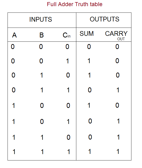
Half Adder Logic Diagram And Truth Table : Half Adder An Overview Sciencedirect Topics : Learn what a half adder is, see the circuit behind it, and a truth table for a half adder.. In previous tutorial of half adder circuit construction, we had seen how computer uses single bit binary numbers 0 and 1 for addition and create sum and in the above image, instead of block diagram, actual symbols are shown. Truth table for the full adder. C out logic diagram for the full adder. The four bit parallel adder is a very common logic circuit. When both inputs are low then sum and carry will be logic low (0), if any one input is here xor gate ic 7486 and logic and gate ic 7408 are used to construct the half adder circuit, both are quad 2 input logic gate ic.
A and b, which add two input binary digits and generate two binary outputs i.e. So a half adder is simply an xor gate. When both inputs are low then sum and carry will be logic low (0), if any one input is here xor gate ic 7486 and logic and gate ic 7408 are used to construct the half adder circuit, both are quad 2 input logic gate ic. We can draw a block diagram for the single digit adder as follows. It outputs the sum binary bit and a carry binary bit.
Full Adder Circuit Diagram from theorycircuit.com A half adder is a logic circuit used for summing two one bit. A half adder is defined as a basic four terminal digital device which adds two binary input bits. Half adder is used in the arithmetic logic unit of the processor of the computer system for performing arithmetic. Half adder is a combinational logic circuit with two inputs and two outputs. The half adder (ha) circuit has two inputs: The major difference between a half adder and a full adder is the number of input half adder truth table. A simple explanation of a half adder. The operation of the above circuit diagram can be understood more clearly with the help of equation.
Learn what a half adder is, see the circuit behind it, and a truth table for a half adder.
The half adder (ha) circuit has two inputs: This can be implemented using and, or and not gates as the logic functions corresponding to the sum is the xor function, and the function for carry is the and function. Truth table of half adder. Numbers or basically two bits. When both inputs are low then sum and carry will be logic low (0), if any one input is here xor gate ic 7486 and logic and gate ic 7408 are used to construct the half adder circuit, both are quad 2 input logic gate ic. Half adder and full adder. Implementation most popular in digital electronics & logic design. Block diagram of half adder. .with truth table full adder logic circuit we can implement a full adder circuit with the help of two half adder circuits. It has two inputs which receive. An adder is a digital logic circuit in electronics that performs the operation of additions of two number. We can see that the output s is an exor between the input a and the though the implementation of larger logic diagrams is possible with the above full adder logic a simpler symbol is mostly used to represent the operation. This circuit constructed using half adder circuitry it requires two xor gates, two and and one or.
Overcome this constraint, full adders are established. We can quickly calculate what the answers should be The half adder (ha) circuit has two inputs: Here is the truth table. Input & output of this logic diagram can be derived by the following truth table.
2 Practical Assignment 2 Binary Adders The Diode from sites.google.com Truth tables offer a simple and easy to understand tool that can be used to determine the output of any logic gate or circuit for all input combinations. Circuit diagram of half adder using nand gates. Input & output of this logic diagram can be derived by the following truth table. We can draw a block diagram for the single digit adder as follows. A demultiplexer performs the reverse operation of a multiplexer i.e. Half adder is used in the arithmetic logic unit of the processor of the computer system for performing arithmetic. We can quickly calculate what the answers should be .with truth table full adder logic circuit we can implement a full adder circuit with the help of two half adder circuits.
From the truth table, it can be concluded as.
A half adder is used for adding together the two least significant digits in a binary sum such as the one shown in figure 12.1(a). Numbers or basically two bits. We can draw a block diagram for the single digit adder as follows. A demultiplexer performs the reverse operation of a multiplexer i.e. An adder is a digital logic circuit in electronics that performs the operation of additions of two number. We know that adding two numbers will generate the summation of the two as a result. This can be implemented using and, or and not gates as the logic functions corresponding to the sum is the xor function, and the function for carry is the and function. The operation of the above circuit diagram can be understood more clearly with the help of equation. The implementation of larger logic diagrams is possible with the above full adder logic a simpler symbol is mostly used to represent the. A half adder is a logic circuit used for summing two one bit. The cout will be true only if any of the two inputs out of the three are high or at logic 1. Truth table of half adder. Truth table of half adder.
The operation of the above circuit diagram can be understood more clearly with the help of equation. Difference between half adder and full adder. It outputs the sum binary bit and a carry binary bit. Half adder and full adder. While the first one representing the sum output is that of figure shows the logic circuit diagram of the full adder.
Binary Adder And Binary Addition Using Ex Or Gates from www.electronics-tutorials.ws the implementation of larger logic diagrams is possible with full adder logic. Navy electricity and electronics training series neets module. Truth table of the half adder. The four bit parallel adder is a very common logic circuit. A simple explanation of a half adder. When a logic gate has only two inputs, or the logic circuit to be analyzed has only one or two gates, it is fairly easy to remember how a. A demultiplexer performs the reverse operation of a multiplexer i.e. Truth tables offer a simple and easy to understand tool that can be used to determine the output of any logic gate or circuit for all input combinations.
Navy electricity and electronics training series neets module.
Half adder is used in the arithmetic logic unit of the processor of the computer system for performing arithmetic. The operation of the above circuit diagram can be understood more clearly with the help of equation. Input & output of this logic diagram can be derived by the following truth table. So a half adder is simply an xor gate. Half adder is a digital logic circuit that takes two bits in adds them and provides two outputs one sum and one carry. Navy electricity and electronics training series neets module. Ø the output is equal to 1 when. Sum = a xor b carry = a and b. Truth table of half adder. The implementation of larger logic diagrams is possible with the above full adder logic a simpler symbol is mostly used to represent the. the implementation of larger logic diagrams is possible with full adder logic. The four bit parallel adder is a very common logic circuit. Overcome this constraint, full adders are established.